
PCBA Reliability
Singularity Engineering is the unique provider for the full suite of PCBA reliability simulation solutions. We combine the powerful solution capability of ANSYS Mechanical with the ease of use and rich dataset of DFR Sherlock to help customers tackle DFM (Design for manufacturability) and DFR (Design for reliability) concerns early on in the design process.
Solder Joint fatigue
Thermal cycling induced solder joint fatigue has been the main source of electronics failure and the cause for numerous expensive product recalls. Simulation has been used to successfully remedy these issues during the design process for many years.
In addition to detailed BGA fatigue simulations, we offer fast checks for the entire PCBA. This provides time to failure estimates for every component on a PCBA for a basic PCB layout file.
Discovering solder joint failure during physical testing typically results in expensive fixes and months of delays. A quick simulation will significantly reduce your risk.
Shock and Random Vibrations
Mobile and automotive applications have stringent shock and vibration requirements as these are important failure modes to consider. Standard shock and vibration tests will identify failures. However, by the time prototypes are built and tested, any changes are bound to be lengthy and expensive.
We offer shock and vibration simulations that predict time to failure from a PCB layout file. With hundreds of thousands of components in our library, and a vast trove of reliability data, we are uniquely positioned to provide you with the confidence and peace of mind you’d want before you go into physical testing.
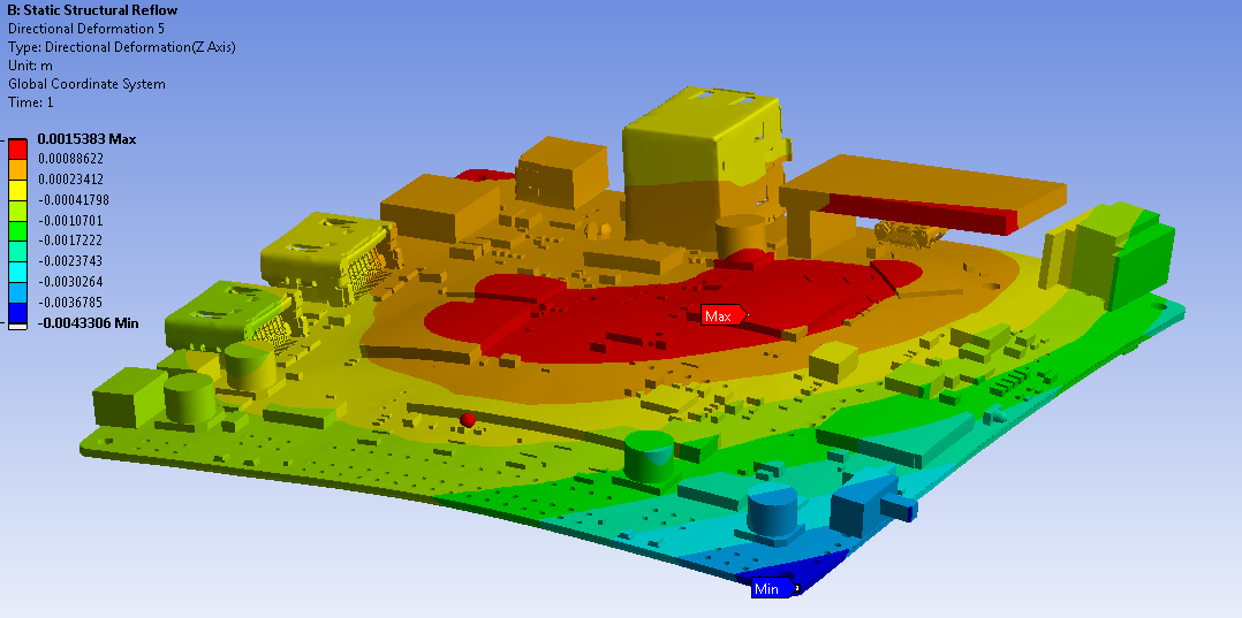
PCBA Warpage
The switch to lead free solder and increasingly thick and complex boards have made the solder reflow process more prone to failure. Due to the excessive warpage induced by large CTE differences, PCBA warpage during reflow can significantly reduce production yield.
We offer specialized tools that allow you to quickly model the entire PCBA, taking into account the details of the trace distribution for each layer of the PCB. This allows simulations to accurately capture PCBA warpage from a simple PCB layout, allowing you to identify issues before they arise.